| XC3000 | XC4000E | XC4000X | XC5200 | XC9000 | Spartan | SpartanXL | Virtex |
|---|---|---|---|---|---|---|---|
| Macro | Macro | Macro | Macro | Macro | Macro | Macro | Macro |
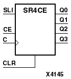
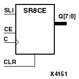
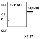
SR4CE, SR8CE, and SR16CE are 4-, 8-, and 16-bit shift registers, respectively, with a shift-left serial input (SLI), parallel outputs (Q), and clock enable (CE) and asynchronous clear (CLR) inputs. The CLR input, when High, overrides all other inputs and resets the data outputs (Q) Low. When CE is High and CLR is Low, the data on the SLI input is loaded into the first bit of the shift register during the Low-to-High clock (C) transition and appears on the Q0 output. During subsequent Low-to-High clock transitions, when CE is High and CLR is Low, data is shifted to the next highest bit position as new data is loaded into Q0 (SLI![]() Q0, Q0
Q0, Q0![]() Q1, Q1
Q1, Q1![]() Q2, and so forth). The register ignores clock transitions when CE is Low.
Q2, and so forth). The register ignores clock transitions when CE is Low.
Registers can be cascaded by connecting the last Q output (Q3 for SR4CE, Q7 for SR8CE, or Q15 for SR16CE) of one stage to the SLI input of the next stage and connecting clock, CE, and CLR in parallel.
The register is asynchronously cleared, outputs Low, when power is applied. For CPLDs, the power-on condition can be simulated by applying a High-level pulse on the PRLD global net. FPGAs simulate power-on when global reset (GR) or global set/reset (GSR) is active. GR for XC3000 is active-Low. GR for XC5200 and GSR (XC4000, Spartans, Virtex) default to active-High but can be inverted by adding an inverter in front of the GR/GSR input of the STARTUP or STARTUP_VIRTEX symbol.
| Inputs | Outputs | ||||
|---|---|---|---|---|---|
| CLR | CE | SLI | C | Q0 | Qz - Q1 |
| 1 | X | X | X | 0 | 0 |
| 0 | 0 | X | X | No Chg | No Chg |
| 0 | 1 | 1 | 1 | qn-1 | |
| 0 | 1 | 0 | 0 | qn-1 | |
| z = 3 for SR4CE; z = 7for SR8CE; z = 15 for SR16CE qn-1 = state of referenced output one setup time prior to active clock transition | |||||
Figure 10.4 SR8CE Implementation XC3000, XC4000, XC5200, XC9000, Spartans, Virtex |