|
|
|
|
|
|
| XC3000 | XC4000E | XC4000X | XC5200 | XC9000 | Spartan | SpartanXL | Spartan2 | Virtex |
|---|---|---|---|---|---|---|---|---|
| N/A | Macro | Macro | N/A | N/A | Macro | Macro | Macro | Macro |
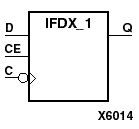
The IFDX_1 D-type flip-flop is contained in an input/output block (IOB). The input (D) of the flip-flop is connected to an IPAD or an IOPAD. The D input also provides data input for the flip-flop, which synchronizes data entering the chip. The data on input D is loaded into the flip-flop during the High-to-Low clock (C) transition and appears at the output (Q). The clock input can be driven by internal logic or through another external pin. When the CE pin is Low, the output (Q) does not change.
The flip-flop is asynchronously cleared with Low output, when power is applied. FPGAs simulate power-on when global set/reset (GSR) is active. GSR defaults to active-High but can be inverted by adding an inverter in front of the GSR input of the STARTUP, STARTUP_SPARTAN2, or STARTUP_VIRTEX symbol.
For information on legal IFDX, IFDX_1, ILDX, and ILDX_1 combinations, refer to the “ILDX, 4, 8, 16” section.
| Inputs | Outputs | ||
|---|---|---|---|
| CE | D | C | Q |
| 1 | D | d | |
| 0 | X | X | No Chg |
| d = state of D input one setup time prior to active clock transition | |||