|
|
|
|
|
|
| XC3000 | XC4000E | XC4000X | XC5200 | XC9000 | Spartan | SpartanXL | Spartan2 | Virtex |
|---|---|---|---|---|---|---|---|---|
| N/A | N/A | N/A | N/A | N/A | N/A | N/A | Primitive | Primitive |
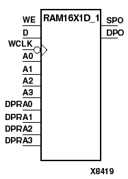
RAM16X1D_1 is a 16-word by 1-bit static dual port random access memory with synchronous write capability and negative-edge clock. The device has two separate address ports: the read address (DPRA3 - DPRA0) and the write address (A3 - A0). These two address ports are completely asynchronous. The read address controls the location of the data driven out of the output pin (DPO), and the write address controls the destination of a valid write transaction.
When the write enable (WE) is Low, transitions on the write clock (WCLK) are ignored and data stored in the RAM is not affected. When WE is High, any negative transition on WCLK loads the data on the data input (D) into the word selected by the 4-bit write address. For predictable performance, write address and data inputs must be stable before a High-to-Low WCLK transition. This RAM block assumes an active-High WCLK. WCLK can be active-High or active-Low. Any inverter placed on the WCLK input net is absorbed into the block.
You can initialize RAM16X1D_1 during configuration. See “Specifying Initial Contents of a RAM” in the “RAM16X1” section.
Mode selection is shown in the following truth table.
| Inputs | Outputs | |||
|---|---|---|---|---|
| WE (mode) | WCLK | D | SPO | DPO |
| 0 (read) | X | X | data_a | data_d |
| 1 (read) | 0 | X | data_a | data_d |
| 1 (read) | 1 | X | data_a | data_d |
| 1 (write) | D | D | data_d | |
| 1 (read) | X | data_a | data_d | |
| data_a = word addressed by bits A3-A0 data_d = word addressed by bits DPRA3-DPRA0 | ||||
The SPO output reflects the data in the memory cell addressed by A3 - A0. The DPO output reflects the data in the memory cell addressed by DPRA3 - DPRA0.
Note: The write process is not affected by the address on the read address port.