
OFDX_1
Output D Flip-Flop with Inverted Clock and Clock Enable
XC3000
| XC4000E
| XC4000X
| XC5200
| XC9000
| Spartan
| SpartanXL
| Virtex
|
|---|
N/A
| Macro
| Macro
| N/A
| N/A
| Macro
| Macro
| Macro
|
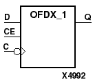
OFDX_1 is located in an input/output block (IOB). The output (Q) of the D flip-flop is connected to an OPAD or an IOPAD. The data on the D input is loaded into the flip-flop during the High-to-Low clock (C) transition and appears on the Q output. When the CE pin is Low, the output (Q) does not change.
The flip-flop is asynchronously cleared with Low output when power is applied. FPGAs simulate power-on when global set/reset (GSR) is active. GSR (XC4000, Spartans) default to active-High but can be inverted by adding an inverter in front of the GSR input of the STARTUP symbol.
Inputs
| Outputs
|
|---|
CE
| D
| C
| Q
|
|---|
1
| D
| 
| d
|
0
| X
| X
| No Chg
|
d = state of referenced input one setup time prior to active clock transition
|
