|
|
|
|
|
|
| XC3000 | XC4000E | XC4000X | XC5200 | XC9000 | Spartan | SpartanXL | Spartan2 | Virtex |
|---|---|---|---|---|---|---|---|---|
| N/A | N/A | Primitive | N/A | N/A | N/A | Primitive | N/A | N/A |
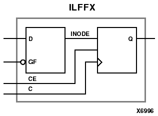
ILFFX, an optional latch that drives the input flip-flop, allows the very fast capture of input data. Located on the input side of an IOB, the latch is latched by the output clock - the clock used for the output flip-flop - rather than the input clock. Thus, two different clocks can be used to clock the two input storage elements. The following figure shows an example IOB block diagram of the XC4000X IOB. After the data is captured, it is then synchronized to the internal clock (C) by the IOB flip-flop.
The latch input (D) is connected to an IPAD or an IOPAD (without using an IBUF). When the gate input (GF) is Low, the data at the input (D) appears at INODE and is stored during the Low-to-High GF transition. The captured INODE data appears at output (Q) during a Low-to-High clock (C) transition.
The fast latch is asynchronously cleared when power is applied. FPGAs simulate power-on when global set/reset (GSR) is active. GSR defaults to active-High but can be inverted by adding an inverter in front of the GSR input of the STARTUP symbol.
| Inputs | Outputs | |||
|---|---|---|---|---|
| CE | D | GF | C | Q |
| 0 | X | X | X | No Chg |
| 1 | X | 1 | INODE | |
| 1 | 0 | 0 | 0 | |
| 1 | 1 | 0 | 1 | |