Libraries GuideChapter 8: Design Elements (OAND2 to OXOR2)
OFDEI_1
D Flip-Flop with Active-High Enable Output Buffer and Inverted Clock (Asynchronous Preset)
XC3000
| XC4000E
| XC4000X
| XC5200
| XC9000
| Spartan
| SpartanXL
| Spartan2
| Virtex
|
|---|
N/A
| Macro
| Macro
| N/A
| N/A
| Macro
| Macro
| N/A
| N/A
|
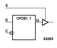
OFDEI_1 and its output buffer exist in an input/output block (IOB). The data output of the flip-flop (Q) is connected to the input of an output buffer or OBUFE. The output of the OBUFE is connected to an OPAD or an IOPAD. The data on the data input (D) is loaded into the flip-flop on the High-to-Low clock (C) transition. When the active-High enable input (E) is High, the data on the flip-flop output (Q) appears on the O output. When E is Low, the output is high impedance (Z state or off).
The flip-flop is asynchronously preset, output High, when power is applied. FPGAs simulate power-on when global set/reset (GSR) is active. GSR defaults to active-High but can be inverted by adding an inverter in front of the GSR input of the STARTUP symbol.
Inputs
| Outputs
|
|---|
E
| D
| C
| O
|
|---|
0
| X
| X
| Z
|
1
| 1
| 
| 1
|
1
| 0
|
| 0
|