|
|
|
|
|
|
The output of PAR is a placed and routed NCD file (the output design file). In addition to the output design file, a PAR run generates a report file with a .par extension, a delay file with a .dly extension, and a pinout file with a .pad extension. The PAR file contains execution information about the place and route job as well as all constraint messages. The DLY file contains delay information about the routed nets in the design. The PAD file lists IOBs (Input/Output Blocks) on the chip and the primary pins associated with the IOBs.
If the options that you specify when running PAR are options that produce a single output design file, your output is the output design file, a PAR file, a DLY file, and a PAD file. The PAR file, the DLY file, and the PAD file all have the same root name as the output design file.
If you run multiple iterations of placement and routing, you produce an output design file, a PAR file, a DLY file, and a PAD file for each iteration. Consequently, when you run multiple iterations you have to specify a directory in which to place these files.
As the command is performed, PAR records a summary of all placement and routing iterations in one PAR file at the same level as the directory you specified, then places the output files (in NCD format) in the specified directory. Also, a PAR file, a DLY file, and a PAD file are created for each NCD file, describing in detail each individual iteration.
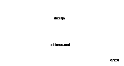
For example, suppose you have a directory named design with a design file called address.ncd, as shown in the following figure.
Suppose you run three iterations of place and route, using a different cost table entry each time (cost tables are explained in the “Placement” section) and specify that the resulting output be put into a directory called output.dir. The actual command would be
par -n 3 -l 1 address.ncd output.dir
-n 3 is the number of iterations you want to run, -l 1 sets the placement effort level, address.ncd is your input design file, and output.dir is the name of the directory in which you want to place the results of the PAR run.
The files resulting from the command are shown in the following figure.
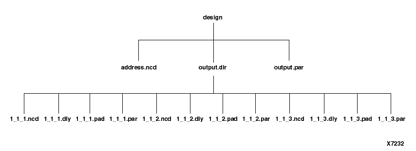
The naming convention for the files, which may contain placement and routing information in varying degrees of completion, is placer_level_router_level_table.file_extension.
In the sample above, the effort level and cost table entries start at 1 (the default value). The PAR, DLY, and PAD files are described in the following sections. When you run multiple iterations, you get a summary PAR report file like the one shown below.
Note: The PAR Report is formatted for viewing in a monospace (non-proportional) font. If the text editor you use for viewing the report uses a proportional font, the columns in the report do not line up correctly.
PAR: Xilinx Place And Route 2.1i.

Copyright (c) 1995-1999 Xilinx, Inc.  All rights reserved.


Mon Mar 15 09:20:46 1999


par -ol 3 -n 5 -i 20 main_pcb.ncd main_pcb.pcf


Constraints file: main_pcb.pcf.


Level/      Design      Timing      Number      Run         NCD

Cost [ncd]  Score       Score       Unrouted    Time        Status

----------  ------      --------    --------    -----       ------------

3_3_1   *   716         0           0           01:02       Complete

3_3_5   *   724         0           0           01:08       Complete

3_3_2   *   730         0           0           01:05       Complete

3_3_4   *   812         0           0           01:06       Complete

3_3_3   *   827         0           0           01:13       Complete


* : Design saved.


par done!
At the top of the summary PAR file is information regarding the software level, copyright information, and the date and time of the run. Directly below that is the command line used to run PAR, followed by the name of any physical constraints file used.
The body of the report consists of the following columns.
Level/Cost [ncd] - indicates the effort level (1-5) at which PAR is run. In the sample above, 3_3_4 indicates placer level 3, router level 3, and the fourth cost table used.
Design Score - see “The Place and Route (PAR) Report File” section.
Timing Score - see “The Place and Route (PAR) Report File” section.
Number Unrouted - indicates the number of unrouted nets in the design.
Run Time - the time required to complete the job in minutes and seconds.
NCD Status - describes the state of the output NCD file generated by the PAR run. Possible values for this column are
PAR generates an intermediate failing timespec summary only in the routing phase. The summary name is design_name.itr.
The router creates this summary after an iteration not during an iteration. If interrupted during normal operation of an iteration (for example, CTRL-C), you are prompted with the following options if a time specification has failed:
CNTRL-C interrupt detected.
Please choose one of the following options:

1. Continue processing and ignore the interrupt.
2. Normal program exit at next check point.
This will result in saving the best results so far,
after concluding current processing.
3. Exit program immediately.
4. Display Failing Timespec Summary.
5. Cancel the current job and move to the next one at

   the next check point.
Enter choice -->
If you select 3. PAR exits. If you select 4, PAR displays the contents of the ITR file on the screen and resumes execution. (Option 5 allows you to terminate jobs that use the -n option for multiple iterations.) If Options 4 and 5 are not applicable, the following messages displays for those options on a CTRL C instead of the ones shown previously.
4. Display Failing Timespec Summary.

   (Not applicable: Data not available)

5. Cancel the current job and move to the next one at

   the next check point.

   (Not applicable: Not a multi-run job.)
Following is a sample ITR report.
Asterisk (*) preceding a constraint indicates it was not met.


----------------------------------------------------------------

  Constraint                                | Requested  | Actual     | Logic

                                            |            |            | Levels

-------------------------------------------------------------------------

* OFFSET = OUT 15 nS  AFTER COMP "ck1_i"    | 15.000ns   | 15.800ns   | 5

-------------------------------------------------------------------------


1 constraint not met.
PAR creates an intermediate failing timespec summary generated from the end of the previous iteration. If the interrupt occurred during the first iteration, no intermediate summary is created.
The place and route (PAR) report file contains execution information about the PAR command run. The file shows the steps taken as the program converges on a placement and routing solution. A sample PAR file is shown following.
Note: The PAR Report is formatted for viewing in a monospace (non-proportional) font. If the text editor you use for viewing the report uses a proportional font, the columns in the report do not line up correctly.
PAR: Xilinx Place And Route 2.1i.

Copyright (c) 1995-1999 Xilinx, Inc.  All rights reserved.

Fri Mar 12 12:09:28 1999


par -w testclk.ncd testclk.ncd


Constraints file: testclk.pcf.


Loading device database for application par from file "testclk.ncd".

   "test_clock" is an NCD, version 2.28, device xcv100, package bg256, speed -5

Loading device for application par from file 'v100.nph' in environment

/build/bcxfndry/C.13/rtf.

Device speed data version:  "x1_0.71 1.76 Advanced".


Device utilization summary:


   Number of External GCLKIOBs         2 out of 4      50%

   Number of External IOBs             4 out of 180     2%


   Number of SLICEs                   64 out of 1200    5%


   Number of GCLKs                     2 out of 4      50%


Overall effort level (-ol):   2 (default)

Placer effort level (-pl):    2 (default)

Placer cost table entry (-t): 1

Router effort level (-rl):    2 (default)

Timing method (-kpaths|-dfs): kpaths (default)


Starting initial Timing Analysis.  REAL time: 5 secs

Finished initial Timing Analysis.  REAL time: 7 secs


Starting initial Placement phase. REAL time: 8 secs

Control signal source res_i

Finished initial Placement phase. REAL time: 8 secs

Starting the placer. REAL time: 8 secs

Placement pass 1 ...

Placer score = 7420

Optimizing ...

Placer score = 5963

Starting IO Improvement.  REAL time: 8 secs

Placer score = 5211

Finished IO Improvement.  REAL time: 8 secs


Placer completed in real time: 8 secs


Total REAL time to placer completion: 8 secs

Total CPU time to placer completion: 5 secs


0 connection(s) routed; 380 unrouted.

Starting router resource preassignment

Completed router resource preassignment. REAL time: 10 secs

Starting iterative routing.

Routing active signals.

End of iteration 1

380 successful; 0 unrouted; (0) REAL time: 12 secs

Constraints are met.

Routing PWR/GND nets.

Power and ground nets completely routed.

Total REAL time: 12 secs

Total CPU  time: 8 secs

End of route.  380 routed (100.00%); 0 unrouted.

No errors found.

Completely routed.


Total REAL time to router completion: 13 secs

Total CPU time to router completion: 8 secs


Generating "par" statistics.


   The Delay Summary Report


   The SCORE FOR THIS DESIGN is: 264


The NUMBER OF SIGNALS NOT COMPLETELY ROUTED for this design is: 0


   The AVERAGE CONNECTION DELAY for this design is:        1.958

   The MAXIMUM PIN DELAY IS:                               6.466

   The AVERAGE CONNECTION DELAY on the 10 WORST NETS is:   3.445


   Listing Pin Delays by value: (nsec)


    d < 1.00   < d < 2.00  < d < 3.00  < d < 4.00  < d < 7.00  d >= 7.00

   ---------   ---------   ---------   ---------   ---------   ---------

          87         165          70          18          40           0


Timing score: 0


Asterisk (*) preceding a constraint indicates it was not met.


-------------------------------------------------------------------------

  Constraint                                | Requested  | Actual     | Logic

                                            |            |            | Levels

-------------------------------------------------------------------------

  TS_ck1_i = PERIOD TIMEGRP "ck1_i"  20 nS  | 20.000ns   | 14.655ns   | 12

    HIGH 50.000 %                           |            |            |

-------------------------------------------------------------------------

  TS_ck2_i = PERIOD TIMEGRP "ck2_i"  18 nS  | 18.000ns   | 14.813ns   | 11

    HIGH 50.000 %                           |            |            |

-------------------------------------------------------------------------

  OFFSET = IN 20 nS  BEFORE COMP "ck1_i"    | 20.000ns   | 6.202ns    | 2

-------------------------------------------------------------------------

  OFFSET = OUT 18 nS  AFTER COMP "ck1_i"    | 18.000ns   | 16.691ns   | 5

-------------------------------------------------------------------------

  OFFSET = IN 22 nS  BEFORE COMP "ck2_i"    | 22.000ns   | 5.861ns    | 2

-------------------------------------------------------------------------

  OFFSET = OUT 17 nS  AFTER COMP "ck2_i"    | 17.000ns   | 14.969ns   | 5

-------------------------------------------------------------------------


All constraints were met.
Sometimes the design is completely routed, but the router continues to route in the attempt to meet timing constraints.
Note that in the sample PAR file above, in the “starting iterative routing” section, after the end of iteration 1, there is a figure in parentheses (0). This represents the timing score for the design (not to be confused with the PAR score) at the end of the particular iteration. This figure appears in the PAR file only when timing constraints have been specified in a PCF file. When the timing score is 0 (as it is in this example after iteration 1), this means that all timing constraints have been met. This score (0) also appears at the end of the delay report section of the PAR file.
The timing score at the end of the “starting iterative routing” section may not agree with the timing score in the Delay Summary Report. This can occur if a MAXSKEW constraint is scored and not met.
Had the design been completely routed but failed to meet all timing constraints, the score would have been a figure other than 0. A non-zero number would appear at the end of the delay report section. This tells you immediately whether your timing constraints have been met. It is possible that the timing score shown in parentheses at the top of the file may be different from the one shown in the delay summary section of the file. The score shown in the delay summary section is always the correct one.
The last section of the PAR file contains a summary of the delay information for the routed design. The DLY (delay) file produced by the PAR run contains more detailed timing information. The DLY file is discussed in the following section.
If you specify a command option that produces multiple output design files, there is a PAR file indicating all of the place and route iterations performed, and individual PAR files describing placement and routing for each design file produced.
Note: In PAR reporting, a tilde (~) preceding a delay value indicates that the delay value is approximate. Values with the tilde cannot be calculated exactly because of excessive delays, resistance, or capacitance on the net. You can use the PENALIZE TILDE constraint to penalize these delays by a specified percentage (see the “TRACE” chapter and the “Attributes, Constraints, and Carry Logic” chapter of the Libraries Guide for a description of the PENALIZE TILDE constraint).
Some notes about the entries in the PAR file.
For the Virtex and Spartan2 devices, if more than one SelectIO standard is used, an additional section on Select IO utilization and usage summary is added to the PAR file. This section shows details for the different IO banks. It shows the IO standard, the output reference voltage (VCCO)] for the bank, the input reference voltage (VREF) for the bank, the PAD and Pin names. In addition, the section gives a summary for each bank with the number of pads being used, the voltages of the VREFs, and the VCCOs. A sample Select IO utilization and Usage Summary of the PAR file follows.
Select IO Utilization and Usage Summary
_______________________________________
NR - means Not Required.

Each Group of a specific Standard is listed.
IO standard (LVTTL Vref=NR Vcco=3.30) occupies 45 pads.
IO standard (CTT Vref=1.50 Vcco=3.30) occupies 8 pads.
IO standard (SSTL3_I Vref=0.90 Vcco=3.30) occupies 12 pads.
Bank Summary

____________

NR - means Not Required

Bank 0 has 20 pads and is 80% utilized.

Vref should be set to NR volts.

Vcco should be set to 3.30 volts.
     Name                IO  Select Std Vref   Vcco   Pad   Pin

     ----                --  ---------- ------ ------ ------ ------

     bidir<7>            IO  LVTTL      NR     3.30   PAD2   P238

     bidir<6>            IO  LVTTL      NR     3.30   PAD3   P237

     bidir<3>            IO  LVTTL      NR     3.30   PAD8   P231

     bidir<1>            IO  LVTTL      NR     3.30   PAD10  P230

     b<10>               I   LVTTL      NR            PAD11  P229

     .

     .

     .

     b<7>                I   LVTTL      NR            PAD17  P221

     a<10>               I   LVTTL      NR            PAD18  P220
Bank 1 has 22 pads and is 13% utilized.

Vref should be set to NR volts.
     Name                IO  Select Std Vref   Vcco   Pad   Pin

     ----                --  ---------- ------ ------ ------ ------

     .

     .

     .

Bank 7 has 21 pads and is 38% utilized.

Vref should be set to 0.90 volts.

Vref sites in this bank cannot be used for user IOBs.

Vcco should be set to 3.30 volts.
     Name                IO  Select Std Vref   Vcco   Pad   Pin

     ----                --  ---------- ------ ------ ------ ------

     bidir<11>           IO  SSTL3_I    0.90   3.30   PAD169 P28

     bidir<8>            IO  SSTL3_I    0.90   3.30   PAD170 P27

     bidir<9>            IO  SSTL3_I    0.90   3.30   PAD172 P25

     bidir<10>           IO  SSTL3_I    0.90   3.30   PAD173 P24

     c<9>                O   CTT               3.30   PAD181 P13

     c<10>               O   CTT               3.30   PAD187 P7

     c<7>                O   LVTTL             3.30   PAD190 P4

     c<8>                O   CTT               3.30   PAD191 P3
Total REAL time to Placer completion: 40 secs

Total CPU time to Placer completion: 31 secs
For guided par, the PAR report displays summary information describing the total amount and percentage of components and signals in the input design guided by the reference design. The report also displays the total/percentage of components and signals from the reference design (guide file) that were used to guide the input design. See the “Guide Reporting” section.
The delay file is output by each PAR run and is placed in the directory with the NCD output of the design file and the PAR file. The delay file contains delay information for each net in the design and includes the following:
The following is a portion of a delay file. If this were a complete file, it would show the load delays for all nets in the design.
Note: The Delay Report is formatted for viewing in a monospace (non-proportional) font. If the text editor you use for viewing the report uses a proportional font, the columns in the report do not line up correctly.
Fri Mar 12 12:09:41 1999


File: testclk.dly


The 20 worst nets by delay are:

-------------------------------

| Max Delay       | Netname   |

-------------------------------

   6.466            res

   4.513            core_inst2/counter1/C54/N32

   3.985            out1

   3.577            core_inst1/counter1/C9/N32

   3.103            core_inst2/counter1/cont<8>

   3.073            core_inst1/counter1/cont<1>

   3.061            start

   2.908            core_inst2/counter1/cont<4>

   2.844            core_inst2/counter1/cont<2>

   2.832            core_inst1/counter1/cont<8>

   2.589            core_inst2/counter1/cont<9>

   2.572            core_inst2/counter1/cont<3>

   2.343            syn2548

   2.281            core_inst1/counter1/cont<3>

   2.260            core_inst2/counter1/regist0<2>

   2.247            core_inst1/counter1/cont<0>

   2.184            core_inst2/counter1/regist0<8>

   2.160            core_inst1/counter1/regist0<9>

   2.156            core_inst1/counter1/regist0<1>

   2.149            core_inst2/counter1/cont<5>

---------------------------------


------------------------------------------------------------------

                               Net Delays

------------------------------------------------------------------


N_ck1_i

   ck1_i.GCLKOUT

         0.001  BUFG_ck1.IN


N_ck2_i

   ck2_i.GCLKOUT

         0.001  BUFG_ck2.IN


ck1

   BUFG_ck1.OUT

         1.003  core_inst1/counter1/regist0<6>.CLK

         0.992  core_inst1/counter1/regist1<0>.CLK

         1.003  core_inst1/counter1/regist1<8>.CLK

.

.

.
The PAD file contains a listing of all IOBs used in the design and their associated pads. The file specifies connections to device pins (with a P prefix).
The PAD file is divided into three sections.
For 2.1i, the PAD file reports all dual-purpose pins that are used during configuration as well during normal operation.
A sample PAD file is shown following.
Note: The PAD Report is formatted for viewing in a monospace (non-proportional) font. If the text editor you use for viewing the report uses a proportional font, the columns in the report do not line up correctly.
PAR: Xilinx Place And Route 2.1i.

Copyright (c) 1995-1999 Xilinx, Inc.  All rights reserved.

Fri Mar 12 12:09:43 1999


Xilinx PAD Specification File

*****************************


INPUT FILE:       testclk.ncd

OUTPUT FILE:      testclk.ncd

PART TYPE:        xcv100

SPEED GRADE:      -5

PACKAGE:          bg256


Fri Mar 12 12:09:43 1999


Pinout by Pin Name:

+------------------------------------------------+-----------+----------+

|                    Pin Name                    | Direction |  Pin Number  |

+------------------------------------------------+-----------+----------+

| ck1_i                                          |  INPUT    | B10          |

| ck2_i                                          |  INPUT    | Y10          |

| out1_o                                         |  OUTPUT   | Y7           |

| out2_o                                         |  OUTPUT   | V8           |

| res_i                                          |  INPUT    | Y9           |

| start_i                                        |  INPUT    | A7           |

+------------------------------------------------+-----------+----------+

|                Dedicated or Special Pin Name               |  Pin Number  |

+------------------------------------------------------------+----------+

| CCLK                                                       | B19          |

| CS                                                         | B18          |

| D1                                                         | E20          |

.                                                          .

.                                                          .

.                                                          .

| VCCO_6                                                     | P4           |

| VCCO_7                                                     | H4           |

| VCCO_7                                                     | G4           |

| WRITE                                                      | A19          |

+------------------------------------------------------------+----------+


Pinout by Pin Number:

+--------------+-----------------------------------+-----------+--------+

|  Pin Number  |            Pin Name               | Direction | Constraint |

+--------------+-----------------------------------+-----------+--------+

| A1           | (TCK)                             |           |            |

| A2           | ---                               |  UNUSED   |            |

| A3           | ---                               |  UNUSED   |            |

| A4           | ---                               |  UNUSED   |            |

  .                                                          .

  .                                                          .

  .                                                          .

| Y17          | ---                               |  UNUSED   |            |

| Y18          | ---                               |  UNUSED   |            |

| Y19          | ---                               |  UNUSED   |            |

| Y20          | (PROGRAM)                         |           |            |

+--------------+-----------------------------------+-----------+--------+


#

# Pinout constraints listing

# These constraints are in PCF grammar format

# and may be cut and pasted into the PCF file

# after the "SCHEMATIC END ;" statement to

# preserve this pinout for future design iterations.

#

COMP "ck1_i" LOCATE = SITE "Y10" ;

COMP "ck2_i" LOCATE = SITE "B10" ;

COMP "out1_o" LOCATE = SITE "V9" ;

COMP "out2_o" LOCATE = SITE "B9" ;

COMP "res_i" LOCATE = SITE "B5" ;

COMP "start_i" LOCATE = SITE "Y9" ;

#
For the Virtex or Spartan2 devices, when SelectIOs are used, the PAD file also contains details of the pads that must be used for the input reference voltage (VREF), and those that must be used for the output reference voltage (VCCO). For the VREF pads, their location and the value of the input reference voltage is shown. A sample Virtex PAD file follows.
PAR: Xilinx Place And Route 2.1i.

Copyright (c) 1995-1999 Xilinx, Inc.  All rights reserved.

Fri Mar 12 12:09:43 1999


Xilinx PAD Specification File
*****************************
Input file:       virtex_test.ncd

Output file:      virtex_test.out.ncd

Part type:        xcv50

Speed grade:      -5

Package:          pq240
Fri Mar 12 12:09:43 1999
Pinout by Pin Name:

+------------------------------------------------+-----------+----------+

|                   Pin Name                     | Direction |  Pin Number  |

+------------------------------------------------+-----------+----------+

| a<0>                                           |  INPUT    | P97          |

| a<1>                                           |  INPUT    | P99          |

| a<2>                                           |  INPUT    | P103         |

| a<3>                                           |  INPUT    | P113         |

         .

         .

         .

+------------------------------------------------+-----------+----------+

|               Dedicated or Special Pin Name                |  Pin Number  |

+------------------------------------------------------------+----------+

| CCLK                                                       | P179         |

| DONE                                                       | P120         |

| GND                                                        | P14          |

         .

         .

         .

| VCCO                                                       | P197         |

| VCCO                                                       | P105         |

| VREF (0.90V)                                               | P9           |

| VREF (0.90V)                                               | P70          |

| VREF (0.90V)                                               | P84          |

| VREF (1.50V)                                               | P36          |

| VREF (1.50V)                                               | P50          |

+------------------------------------------------------------+----------+

Pinout by Pin Number:

+--------------+-----------------------------------+-----------+--------+

|  Pin Number  |           Pin Name                | Direction | Constraint |

+--------------+-----------------------------------+-----------+--------+

| P1           | GND                               |           |            |

| P2           | TMS                               |           |            |

         .

         .

         .

| P9           | VREF (0.90V)                      |           |            |

| P36          | VREF (1.50V)                      |           |            |

| P61          | VCCO                              |           |            |

+--------------+-----------------------------------+-----------+--------+

#

# Pinout constraints listing

# These constraints are in PCF grammar format

# and may be cut and pasted into the PCF file

# after the "SCHEMATIC END ;" statement to

# preserve this pinout for future design iterations.

#

         .

         .

         .
This report, which is included in the PAR report file, is generated when using the -gf option. The report describes the criteria used to select each component and signal used to guide the design. It may also enumerate the criteria used to reject some subset of the components and signals that were eliminated as candidates.
Following is an example of guide file information that displays in the PAR file.
PAR: Xilinx Place And Route 2.1i.

Copyright (c) 1995-1999 Xilinx, Inc.  All rights reserved.


Mon Mar 15 13:39:04 1999


par -gm leverage -gf g1.ncd testclk.ncd guide.ncd testclk.pcf


Constraints file: testclk.pcf.


Loading device database for application par from file "testclk.ncd".

   "test_clock" is an NCD, version 2.28, device xcv100, package bg256, speed -5

Loading device for application par from file 'v100.nph' in environment

/build/bcxfndry/C.13/rtf.

Device speed data version:  "x1_0.71 1.76 Advanced".


Loading device database for application par from file "g1.ncd".

   "test_clock" is an NCD, version 2.28, device xcv100, package bg256, speed -5


Starting guide file placement.


Guide file processing done.


Guide Summary Report:


   Components:     69 out of    72   96%

   Signals:       330 out of   335   99%


   Guide File Components:     69 out of    71   97%

   Placed Guide File Components:     69 out of    69  100%

   Guide File Signals:       330 out of   330  100%


Guide Detail Report:


Guided comps (Guide Comp) located in the guided site:

   Comp syn2469 (syn2469) guided to site CLB_R20C11.S1.

   - Comp successfully guided in matching guide site.

   - Comp names match in both current and guide design.

   - Comp pins have compatible assignements.

   Comp core_inst2/counter1/C54/C5/C1/O (core_inst2/counter1/C54/C5/C1/O)

guided to site CLB_R19C11.S0.

   - Comp successfully guided in matching guide site.

Guided comps (Guide comp) unable to be located in the guided site:


Device utilization summary:


   Number of External GCLKIOBs         2 out of 4      50%

   Number of External IOBs             4 out of 180     2%


   Number of SLICEs                   64 out of 1200    5%


   Number of GCLKs                     2 out of 4      50%