|
|
|
|
|
|
| XC3000 | XC4000E | XC4000X | XC5200 | XC9000 | Spartan | SpartanXL | Spartan2 | Virtex |
|---|---|---|---|---|---|---|---|---|
| Macro | Macro | Macro | Macro | N/A | Macro | Macro | Macro | Macro |
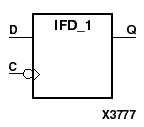
The IFD_1 D-type flip-flop is contained in an input/output block (IOB) except for XC5200. The input (D) of the flip-flop is connected to an IPAD or an IOPAD. The D input also provides data input for the flip-flop, which synchronizes data entering the chip. The D input data is loaded into the flip-flop during the High-to-Low clock (C) transition and appears at the output (Q). The clock input can be driven by internal logic or through another external pin.
The flip-flop is asynchronously cleared with Low output when power is applied. FPGAs simulate power-on when global reset (GR) or global set/reset (GSR) is active. GR for XC3000 is active-Low. GR for XC5200 and GSR (XC4000, Spartans, Virtex) default to active-High but can be inverted by adding an inverter in front of the GR/GSR input of the STARTUP, STARTUP_SPARTAN2, or STARTUP_VIRTEX symbol.
For information on legal IFD, IFD_1, ILD, and ILD_1 combinations, refer to the “ILD, 4, 8, 16” section.
| Inputs | Outputs | |
|---|---|---|
| D | C | Q |
| 0 | 0 | |
| 1 | 1 | |